ED-3-1-INV
In-Plane Tunnel Spectroscopy of Cuprate Superconductors with Nano-Scale Josephson Junctions
15:00-15:30 28/11/2023
*Shane Cybart
Department of Electrical & Computer Engineering
University of California Riverside
Riverside, California, 92521 USA
Superconducting tunnel spectroscopy is a powerful technique to directly measure the density of states of materials to study their electrical properties. It has provided a wealth of information about the nature of electrical transport in enigmatic high-transition temperature (high-TC) superconductors, such as the nature of the energy gap and superconducting pair amplitude. Most of these studies have been along the c-axis direction due to difficulties in engineering tunnel devices oriented in other directions. This is unfortunate as the (high-TC) materials are highly anisotropic, and measurements in bulk crystals show that superconductivity is much stronger in the a-b plane. [1]
In 2015 Cybart et al. developed a new approach to a-b plane tunneling utilizing a focused helium ion beam [2] to fabricate Josephson tunnel junctions in YBa2Cu3O7−δ thin films with the transport current residing entirely within the a-b plane [3]. Unlike prior-art metallic barrier high-TC Josephson junctions, these have insulating barriers and exhibit quasi-particle tunneling with well-described energy gaps.[3] This process relies on the sensitivity of high-TC materials to ion irradiation [4]. Increasing irradiation dosage increases resistivity, and TC decreases. The material becomes a disordered insulator for helium irradiation exceeding 3×10¹⁵ ions/cm2.
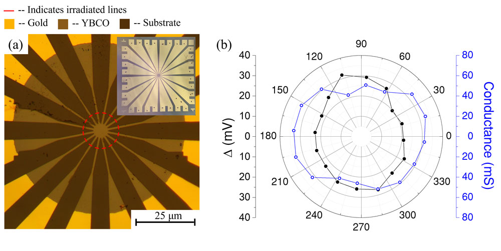
Josephson junctions, a thin film of oxide superconductor, is patterned into electrodes with a thickness of 20-50 nm, and the beam is scanned across to form a narrow ∼1-2 nm disordered insulating region of just a few unit cells. To measure the energy gap Δ of cuprate superconductors, thin films of YBa2Cu3O7 were grown by Ceraco using reactive co-evaporation on single crystal substrates of Al2O3, respectively. A gold contact electrode was subsequently deposited in the same chamber without breaking the vacuum to ensure a low ohmic contact resistance. Laser lithography and argon ion milling were used to pattern electrodes oriented along different crystallographic directions that converged into the center of the chip into a 10 μm circle, as shown in Figure 1(a). Samples were then irradiated with a 36 kV focused helium ion beam that was scanned across each electrode, delivering a dose of approximately 300 ions/nm to create Josephson tunnel junctions.
Differential conductance (dI−dV) was measured for each junction, and 2Δ was defined as the peak. A linear fit was used to estimate the conductance. The results as a function of angle are plotted in Figure 2(b) and show a gap anisotropy with two axes that differ by a factor of roughly 2:1. This is what one would expect from the measurement of bulk detwinned YBCO crystals [1] that show a similar difference between the a and b crystal axes. This measurement suggests a high-quality orientated YBCO film. Furthermore, the conductance is inversely proportional to the gap. In this talk, I will compare and contrast anisotropy measurements for different types of film textures.
[1] J.-T. Kim, J. Giapintzakis, and D. Ginsberg, “Anisotropy of the resistivity in the a- b plane of a superconducting yba 2 cu 3 o 7- δ single crystal,” Journal of superconductivity, vol. 9, pp. 481–484, 1996.
[2] B. W. Ward, J. A. Notte, and N. P. Economou, “Helium ion microscope: A new tool for nanoscale microscopy and metrology,” Journal of Vacuum Science & Technology B: Microelectronics and Nanometer Structures Processing, Measurement, and Phenomena, vol. 24, no. 6, pp. 2871–2874, 2006.
[3] S. A. Cybart, E. Cho, T. Wong, B. H. Wehlin, M. K. Ma, C. Huynh, and R. Dynes, “Nano Josephson superconducting tunnel junctions in YBa2Cu3O7−δ directly patterned with a focused helium ion beam,” Nat. Nanotechnol., vol. 10, no. 7, pp. 598–602, 2015.
[4] A. E. White, K. Short, R. Dynes, A. Levi, M. Anzlowar, K. Baldwin, P. Polakos, T. Fulton, and L. Dunkleberger, “Controllable reduction of critical currents in yba2cu3o7- δ films,” Applied physics letters, vol. 53, no. 11, pp. 1010–1012, 1988.
This work supported by AFOSR and DOE NNSA.
