WB4-3
Asymmetric Critical Current in YBa2Cu3Oy Coated Conductors with a PrBa2Cu3Oy Buffer Layer
Dec.2 09:10-09:25 (Tokyo Time)
Department of Electrical Engineering, Nagoya University, Japan1
Department of Electric and Electronics Engineering, Aichi Institute of Technology, Japan2
Central Research Institute of Electric Power Industry, Japan3
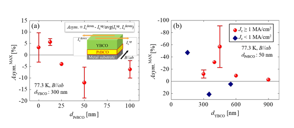
The development of a superconducting diode with different critical currents Ics depending on the current direction has been expected as a novel rectifying element operating at cryogenic conditions [1, 2]. In our previous study, we reported that REBa2Cu3Oy films had an asymmetric Ic which was enhanced by reducing the surface roughness [3]. In this study, focusing on the lattice strain at the bottom interface of YBa2Cu3Oy (YBCO) films, we fabricated YBCO films grown on PrBa2Cu3Oy (PrBCO) buffer layers which have a small lattice mismatch of 0.13 % with YBCO and investigated the asymmetric Ic in the films. Inset of Fig. 1(a) shows a schematic drawing of the films.
The YBCO/PrBCO films were fabricated on IBAD substrates using the pulsed laser deposition method. Thicknesses of PrBCO andYBCO are defined as dPrBCO and dYBCO, respectively. The films were processed into micro bridges. Current-voltage characteristics including the reverse current were measured at 0-0.4 T and 77.3 K by the four-probe method. Inset of Fig. 1(a) shows the definition of current direction and the asymmetricity Asym.. The maximum of the Asym. for the magnetic field is defined as Asym.MAX.
Fig. 1(a) shows dPrBCO dependences of the Asym.MAX in the YBCO/PrBCO films. The Asym.MAX inverted from a positive to a negative with the dPrBCO larger than 12.5 nm. This result indicates that the surface barrier at the bottom interface in the YBCO films is greater than one at the surface. Fig. 1(b) shows dYBCO dependences of the Asym.MAX in the films. The Asym.MAX showed a peak with the maximum value of -103.2 % when the dYBCO was 450 nm, excluding the results with critical current density Jc less than 1 MA/cm2. We will discuss the quantitative analysis of the surface barrier in the films and the structural analysis using a transmission electron microscopy.
This work was partly supported by JSPS-KAKENHI (19K22154, 20K15217, 20H02682), JST-A-STEP, and NEDO. The metal substrates were provided from Dr. Iijima of Fujikura Ltd.
Reference
[1] F. Ichikawa et al.: Physica C 235, 3095-3096 (1994).
[2] S. A. Harrington et al.: Appl. Phys. Lett. 95, 022518 (2009).
[3] Y. Tsuchiya et al.: Abstracts of ISS conference (2019).
Fig. 1(a) PrBa2Cu3Oy layer thickness dPrBCO and (b) YBa2Cu3Oy layer thickness dYBCO dependences of maximum asymmetricity in YBa2Cu3Oy films grown on PrBa2Cu3Oy buffer layers.
Keywords: YBa2Cu3Oy films, critical current Ic, asymmetricity, PrBa2Cu3Oy buffer layers
