ED8-6-INV
Direct-write Printing of Josephson Devices in an Electron Microscope
*Kaveh Lahabi1, Julian Linek2, Timothy van den Berg1, Remko Fermin1, Dieter Kölle2, Reinhold Kleiner2, Tünde de Vries1, Nick Groen1, Jan Aarts1
- Leiden Institute of Physics, Leiden University, the Netherlands1
- Physikalisches Institut and Center for Quantum Science (CQ) in LISA+, Universität Tübingen, Germany2
Josephson devices are the essential building blocks of superconducting electronics. Usually, fabricating a Josephson device is a resource-intensive and multi-step procedure, relying on thin-film deposition and lithography. Moreover, such practices are incompatible with many applications (e.g., non-planar objects and fragile structures). Here, we introduce a fully-additive direct-write approach based on electron beam-induced deposition (EBID), where a conventional scanning electron microscope can print complete Josephson devices in a matter of minutes.
In this talk, I demonstrate that – by tuning the scanning parameter of a focused electron beam – we can print both superconducting (S) and the normal-metal (N) components based on a single material: tungsten carbide. I describe how we utilized this feature to develop printable SNS (proximity) Josephson junctions and SQUIDs with tunable transport characteristics and present an outlook for their applications.
References. [1] T. J. Blom et. al, ACS Nano, 2021, 15, 1, 322–329.
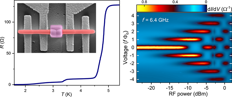
Figure Caption. Left: False colored scanning electron microscope image of a Josephson junction, printed using EBID, and its superconducting transition. Right: Shapiro response of the junction as a function of voltage and external microwave power. The Shapiro steps appear as conductance peaks at quantized voltages
Keywords: Superconducting Devices, Josephson Junction, SQUID, Direct-write Fabrication
